- 您现在的位置:买卖IC网 > Sheet目录2004 > LTC1742CFW#TRPBF (Linear Technology)IC ADC 14BIT 65MSPS 48-TSSOP
2
LTC1742
1742f
PARAMETER
CONDITIONS
MIN
TYP
MAX
UNITS
Resolution (No Missing Codes)
q
14
Bits
Integral Linearity Error
(Note 6)
– 3
±0.75
3
LSB
Differential Linearity Error
q
–1
±0.5
1
LSB
Offset Error
(Note 7)
– 35
±535
mV
Gain Error
External Reference (SENSE = 1.6V)
– 3.5
±1
3.5
%FS
Full-Scale Drift
Internal Reference
±40
ppm/
°C
Full-Scale Drift
External Reference (SENSE = 1.6V)
±20
ppm/
°C
Offset Drift
Internal Reference
±20
V/°C
Input Referred Noise (Transition Noise)
SENSE = 1.6V
0.82
LSBRMS
ORDER PART
NUMBER
OVDD = VDD (Notes 1, 2)
Supply Voltage (VDD) ............................................. 5.5V
Analog Input Voltage (Note 3) .... – 0.3V to (VDD + 0.3V)
Digital Input Voltage (Except OE)
(Note 3) ...................................... – 0.3V to (VDD + 0.3V)
OE Input Voltage (Note 4) ........ – 0.3V to (OVDD + 0.3V)
Digital Output Voltage ................. – 0.3V to (VDD + 0.3V)
OGND Voltage .............................................. – 0.3V to 1V
Power Dissipation ............................................ 2000mW
Operating Temperature Range
LTC1742C ............................................... 0
°C to 70°C
LTC1742I ............................................ – 40
°C to 85°C
Storage Temperature Range ................. – 65
°C to 150°C
Lead Temperature (Soldering, 10 sec).................. 300
°C
LTC1742CFW
LTC1742IFW
TJMAX = 150°C, θJA = 35°C/W
The q indicates specifications which apply over the full operating
temperature range, otherwise specifications are at TA = 25°C. (Note 5)
ABSOLUTE MAXIMUM RATINGS
W
WW
U
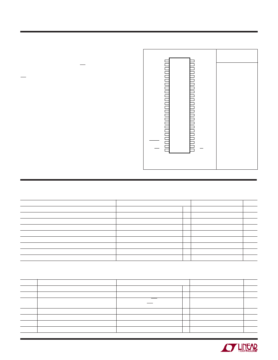
PACKAGE/ORDER INFORMATION
W
U
1
2
3
4
5
6
7
8
9
10
11
12
13
14
15
16
17
18
19
20
21
22
23
24
TOP VIEW
FW PACKAGE
48-LEAD PLASTIC TSSOP
48
47
46
45
44
43
42
41
40
39
38
37
36
35
34
33
32
31
30
29
28
27
26
25
SENSE
VCM
GND
AIN
+
AIN
–
GND
VDD
GND
REFLB
REFHA
GND
REFLA
REFHB
GND
VDD
GND
VDD
GND
MSBINV
ENC
OF
OGND
D13
D12
D11
OVDD
D10
D9
D8
D7
OGND
GND
D6
D5
D4
OVDD
D3
D2
D1
D0
OGND
CLKOUT
OE
CO VERTER CHARACTERISTICS
U
SYMBOL
PARAMETER
CONDITIONS
MIN
TYP
MAX
UNITS
VIN
Analog Input Range (Note 8)
4.75V
≤ VDD ≤ 5.25V
q
±1 to ±1.6
V
IIN
Analog Input Leakage Current
0 < AIN+, AIN– < VDD
q
–1
1
A
CIN
Analog Input Capacitance
Sample Mode ENC < ENC
8
pF
Hold Mode ENC > ENC
4
pF
tACQ
Sample-and-Hold Acquisition Time
q
5
7.3
ns
tAP
Sample-and-Hold Acquisition Delay Time
0
ns
tJITTER
Sample-and-Hold Acquisition Delay Time Jitter
0.15
psRMS
CMRR
Analog Input Common Mode Rejection Ratio
1.5V < (AIN– = AIN+) < 3V
80
dB
The q indicates specifications which apply over the full operating temperature range, otherwise
specifications are at TA = 25°C. (Note 5)
A ALOG I PUT
U
Consult LTC Marketing for parts specified with wider operating temperature ranges.
发布紧急采购,3分钟左右您将得到回复。
相关PDF资料
LTC1743IFW#PBF
IC ADC 12BIT 50MSPS SMPL 48TSSOP
LTC1744IFW#TRPBF
IC ADC 14BIT 50MSPS 48-TSSOP
LTC1745CFW#TRPBF
IC ADC 12BIT 25MSPS LN 48TSSOP
LTC1746IFW#TRPBF
IC ADC 14BIT 25MSPS LP 48TSSOP
LTC1747IFW#PBF
IC ADC 12BIT 80MSPS 48-TSSOP
LTC1748CFW#TRPBF
IC ADC 14BIT 80MSPS 48-TSSOP
LTC1749IFW#PBF
IC ADC 12BIT 80MSPS SMPL 48TSSOP
LTC1750IFW#PBF
IC ADC 14BIT 80MSPS SMPL 48TSSOP
相关代理商/技术参数
LTC1742IFW
功能描述:IC ADC SMPL 14BIT 65MSPS 48TSSOP RoHS:否 类别:集成电路 (IC) >> 数据采集 - 模数转换器 系列:- 标准包装:1 系列:- 位数:14 采样率(每秒):83k 数据接口:串行,并联 转换器数目:1 功率耗散(最大):95mW 电压电源:双 ± 工作温度:0°C ~ 70°C 安装类型:通孔 封装/外壳:28-DIP(0.600",15.24mm) 供应商设备封装:28-PDIP 包装:管件 输入数目和类型:1 个单端,双极
LTC1742IFW#PBF
功能描述:IC ADC 14BIT 65MSPS 48-TSSOP RoHS:是 类别:集成电路 (IC) >> 数据采集 - 模数转换器 系列:- 其它有关文件:TSA1204 View All Specifications 标准包装:1 系列:- 位数:12 采样率(每秒):20M 数据接口:并联 转换器数目:2 功率耗散(最大):155mW 电压电源:模拟和数字 工作温度:-40°C ~ 85°C 安装类型:表面贴装 封装/外壳:48-TQFP 供应商设备封装:48-TQFP(7x7) 包装:Digi-Reel® 输入数目和类型:4 个单端,单极;2 个差分,单极 产品目录页面:1156 (CN2011-ZH PDF) 其它名称:497-5435-6
LTC1742IFW#TR
功能描述:IC ADC SMPL 14BIT 65MSPS 48TSSOP RoHS:否 类别:集成电路 (IC) >> 数据采集 - 模数转换器 系列:- 标准包装:1 系列:- 位数:14 采样率(每秒):83k 数据接口:串行,并联 转换器数目:1 功率耗散(最大):95mW 电压电源:双 ± 工作温度:0°C ~ 70°C 安装类型:通孔 封装/外壳:28-DIP(0.600",15.24mm) 供应商设备封装:28-PDIP 包装:管件 输入数目和类型:1 个单端,双极
LTC1742IFW#TRPBF
功能描述:IC ADC 14BIT 65MSPS 48-TSSOP RoHS:是 类别:集成电路 (IC) >> 数据采集 - 模数转换器 系列:- 标准包装:1 系列:- 位数:14 采样率(每秒):83k 数据接口:串行,并联 转换器数目:1 功率耗散(最大):95mW 电压电源:双 ± 工作温度:0°C ~ 70°C 安装类型:通孔 封装/外壳:28-DIP(0.600",15.24mm) 供应商设备封装:28-PDIP 包装:管件 输入数目和类型:1 个单端,双极
LTC1743CFW
功能描述:IC ADC 12BIT 50MSPS SMPL 48TSSOP RoHS:否 类别:集成电路 (IC) >> 数据采集 - 模数转换器 系列:- 标准包装:1,000 系列:- 位数:12 采样率(每秒):300k 数据接口:并联 转换器数目:1 功率耗散(最大):75mW 电压电源:单电源 工作温度:0°C ~ 70°C 安装类型:表面贴装 封装/外壳:24-SOIC(0.295",7.50mm 宽) 供应商设备封装:24-SOIC 包装:带卷 (TR) 输入数目和类型:1 个单端,单极;1 个单端,双极
LTC1743CFW#PBF
功能描述:IC ADC 12BIT 50MSPS SMPL 48TSSOP RoHS:是 类别:集成电路 (IC) >> 数据采集 - 模数转换器 系列:- 标准包装:1,000 系列:- 位数:12 采样率(每秒):300k 数据接口:并联 转换器数目:1 功率耗散(最大):75mW 电压电源:单电源 工作温度:0°C ~ 70°C 安装类型:表面贴装 封装/外壳:24-SOIC(0.295",7.50mm 宽) 供应商设备封装:24-SOIC 包装:带卷 (TR) 输入数目和类型:1 个单端,单极;1 个单端,双极
LTC1743CFW#TR
功能描述:IC ADC 12BIT 50MSPS SMPL 48TSSOP RoHS:否 类别:集成电路 (IC) >> 数据采集 - 模数转换器 系列:- 标准包装:1,000 系列:- 位数:12 采样率(每秒):300k 数据接口:并联 转换器数目:1 功率耗散(最大):75mW 电压电源:单电源 工作温度:0°C ~ 70°C 安装类型:表面贴装 封装/外壳:24-SOIC(0.295",7.50mm 宽) 供应商设备封装:24-SOIC 包装:带卷 (TR) 输入数目和类型:1 个单端,单极;1 个单端,双极
LTC1743CFW#TRPBF
功能描述:IC ADC 12BIT 50MSPS SMPL 48TSSOP RoHS:是 类别:集成电路 (IC) >> 数据采集 - 模数转换器 系列:- 标准包装:1,000 系列:- 位数:12 采样率(每秒):300k 数据接口:并联 转换器数目:1 功率耗散(最大):75mW 电压电源:单电源 工作温度:0°C ~ 70°C 安装类型:表面贴装 封装/外壳:24-SOIC(0.295",7.50mm 宽) 供应商设备封装:24-SOIC 包装:带卷 (TR) 输入数目和类型:1 个单端,单极;1 个单端,双极